AI COMPUTE•NVIDIA•GPU CLOUD•DATA CENTERS•SEMICONDUCTORS•ENERGY•FUNDING•M&A•AI COMPUTE•NVIDIA•GPU CLOUD•DATA CENTERS•SEMICONDUCTORS•ENERGY•FUNDING•M&A•
Semiconductors

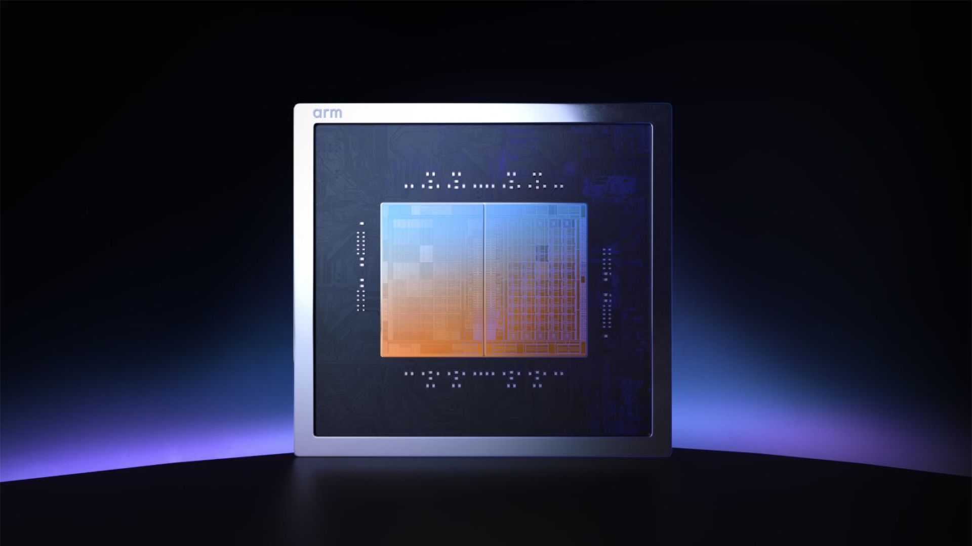
Arm says its AGI CPU delivers nearly 2X the performance per rack of AMD EPYC 9755 in new agentic AI CPU tests

Chip designer claims major rack-density advantage over AMD in server benchmarks
By GPU Data Hub Desk · GPU Data Hub·Editorial standards·
Arm says its AGI CPU delivers nearly 2X the performance per rack of AMD EPYC 9755 in new agentic AI CPU tests

Arm asserts that its AGI CPU provides nearly twice the rack-density performance of AMD's EPYC 9755 across a suite of seven agentic artificial intelligence benchmarks. The findings were derived from a testing standard created in partnership with Meta, OpenAI, and Fujitsu.

Original source

This summary was written by the GPU Data Hub desk from reporting published by Tom's Hardware on 19 Oct 2026, 11:00. Read the full article at the original publisher.

Read Original Source →

By subscribing you consent to receive the daily briefing. Unsubscribe at any time. See our privacy policy.

LinkedInX

More from GPU Data Hub

Latest →

Breaking The Memory Bottleneck In AI And HPC SoCs

Chip architects are refining embedded memory intellectual property to overcome data bottlenecks in high-performance computing and artificial intelligence processors. The design work centres on tailoring memory structures for advanced semiconductor processes, specifically RibbonFET and backside power delivery via PowerVia. These adjustments aim to ensure memory subsystems keep pace with accelerated logic advancements.

Semiconductors··Semiconductor Engineering

Why Physical AI Is So Hard To Engineer

Engineers developing physical artificial intelligence systems face complex silicon design hurdles due to the convergence of distinct hardware domains. Autonomous platforms require the simultaneous integration of compute logic, sensing components, and mechanical actuators on tight performance budgets. Balancing these varied requirements poses unique complications for next-generation edge device architecture.

Semiconductors··Semiconductor Engineering

Shift-Left DE-Via

A shift-left methodology for design-rule-aware via placement aims to produce signoff-ready physical layouts with reduced risk of electrical shorts. By integrating Calibre-aware checks earlier into the design flow, engineers can detect and resolve fabrication vulnerabilities sooner. The technique seeks to improve manufacturing yield and layout reliability in advanced node implementation.

Semiconductors··Semiconductor Engineering